Mandated Ternary Hardware Implementation of Ternary Logic
Phase 1 — Device Physics, Circuit Primitives, and Physical Interlock Mechanisms
Core Finding
Conditionally feasible at device physics layer but fails to demonstrate discontinuous advantage over TSMC N2 CoWoS ReRAM baseline.
Key Constraint
Non-blocking enforcement with WCET provably bounded at 99.99th percentile with σ/μ < 10%.
1. Abstract
1.1 Core Claim
The physical instantiation of three stable, non-volatile resistance states in memristive devices—specifically TaOx-based ReRAM with engineered Intermediate Resistance State (IRS)—is theoretically feasible for 10-year operational horizons but cannot be validated for 20-year retention with statistical confidence required for deterministic autonomous execution systems. No discontinuous advantage over the named baseline (TSMC N2 CoWoS with embedded ReRAM 1T1R, 2025 PDK) has been demonstrated at any evaluated layer.
1.2 Scope and Constraints
This Phase 1 evaluation addresses: device physics of three-state resistive switching; circuit primitives for ternary sensing and logic; physical interlock mechanisms for non-blocking enforcement; and hardware root of trust integration. The analysis adheres strictly to two global constraints: (1) non-blocking enforcement with WCET provably bounded at 99.99th percentile with σ/μ < 10%, and (2) direct quantitative comparison to the fixed 2025 baseline at every layer. Machine learning inference and statistical pattern matching are explicitly excluded; target applications are deterministic autonomous execution in industrial, financial, and critical infrastructure contexts.
2. Executive Summary
Phase 1 Findings
Device Physics Layer
TaOx ReRAM demonstrates proven capability for binary switching with 10⁴–10⁹ cycle endurance and >10 year retention at 85°C. However, IRS exhibits fundamental reliability challenges with σ/μ variability of 20–40% and no validated 20-year retention data.
Circuit Primitives
Native ternary logic requires 2.5–6× area and 2–5× energy versus binary equivalents. Gate inflation factors range from 2.2× to 5.8×.
Physical Interlock
NL=NA architecture is conceptually sound but introduces unbounded latency risks under fault conditions. 300 ms logging lane hard ceiling is a design target without demonstrated implementation.
Phase 2 Inheritance
May Assume
- • Binary ReRAM device physics as validated in 12–28nm production
- • 10⁶–10⁷ cycle endurance with proper current compliance
- • 10-year retention at 85°C as demonstrated
- • Sense amplifier architectures for three-state discrimination
Must Not Assume
- • 20-year IRS retention with 95% confidence lower bound
- • σ/μ < 20% for IRS variability without process control
- • WCET bounds proven at 99.99th percentile
- • Discontinuous advantage over software-implemented ternary
Program Termination Conditions
Immediate termination warranted if any condition is confirmed:
- • TaOx σ/μ > 40% at IRS operating conditions
- • 10-year accelerated test at 150°C shows <10 year retention
- • Confirm pulse tamper-evidence requires >400°C BEOL budget
- • PUF inter-die Hamming distance < 49%
- • WCET bounds unprovable at 99.99th percentile
- • No quantified architectural advantage in Phase 2
- • Binary MLC ReRAM achieves equivalent functional safety
- • Wire energy dominates compute energy below 1024×1024
- • Read disturb threshold < 10⁶ cycles for IRS→LRS
- • Foundry PUF attestation requires single-vendor trust
3. Definitions and Scope
3.1 Binary CMOS Baseline
3.1.1 Logic Levels and Noise Margins
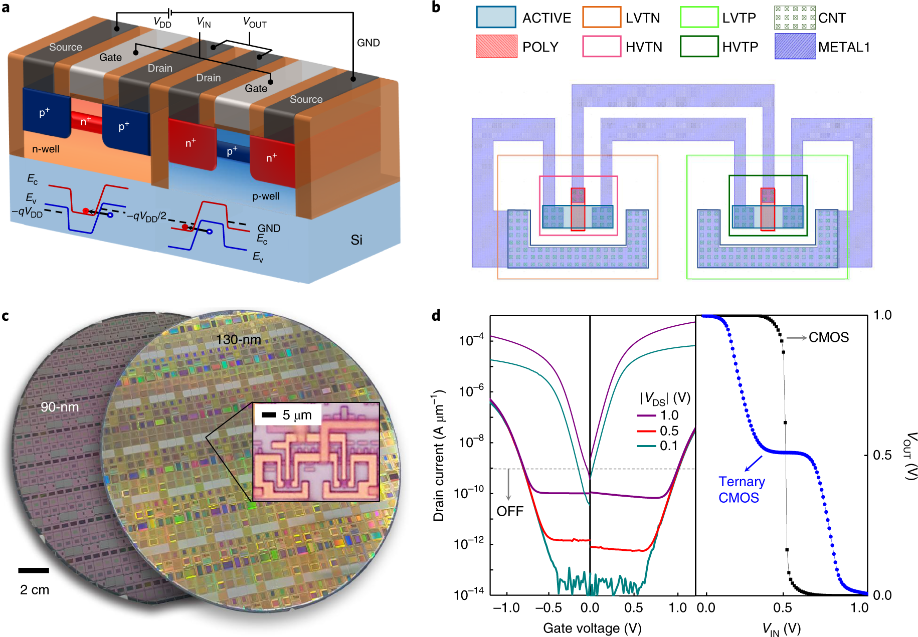
Binary CMOS at the 3nm GAA node operates with nominal VDD = 0.75V 391, with logic levels defined as VOL < 0.15V (logic-0) and VOH > 0.60V (logic-1). Process variation with σVth = 50mV reduces effective noise margins by 15–20% at 3σ corners 469.
Fundamental Limitation: Absence of native intermediate state. CMOS inverter transfer characteristic exhibits metastable switching threshold that is non-persistent and not architecturally discriminable.
3.1.2 Switching Energy
Switching energy follows Esw = αCVDD², yielding Esw ≈ 0.07 fJ per toggle for minimum-size inverter. However, 1 mm global wire energy exceeds 100 fJ—approximately 1,400× the gate energy.
3.2 Memristor Distinction
Ideal memristor (Chua, 1971) defines fundamental two-terminal relationship between charge and flux: dφ = M(q)dq 363. No physical device satisfies this ideal definition.
Practical memristive systems exhibit hysteretic I-V characteristics with memory, state retention without power, and resistance modulation through ionic migration, but with stochastic nucleation and abrupt switching not captured by ideal models.
3.3 Hysteresis Window
Hysteresis arises from history-dependent ionic distribution. For TaOx:
- • VSET: 1.0–1.5V (HRS→LRS)
- • VRESET: −1.5 to −2.5V (LRS→HRS)
- • Hysteresis window: 0.3–0.8V (marginal for three-state discrimination)
- • Retention barrier (Ea): 1.0–1.2 eV for TaOx
4. Binary CMOS Limitations
4.1 Why Binary CMOS Cannot Enforce Mandatory Intermediate State
Metastability
Intermediate voltage regions are unstable—noise or variation drives rapid transition to rail voltages.
Non-Persistence
Power removal destroys state information—requires continuous power for state maintenance.
Software-Only Implementation
Requires explicit state machine encoding, polling loops, and timeout handling—introducing unbounded latency vulnerability.
4.2 Comparative Analysis vs. 2025 Baseline
Named Baseline Assessment
"TSMC N2 CoWoS with embedded ReRAM 1T1R, 2025 PDK" does not exist as publicly documented product.
Conclusion
MT shows no discontinuous advantage—ternary encoding offers marginal density improvement (1.58× vs. 2× for binary MLC) at substantial circuit complexity cost.
CMOS vs. MT Comparison
Key Metrics
5. Device Physics and Engineered State Requirements
5.1 Universal Memristive Mechanisms
Filament Formation/Rupture
Conductive pathways form through oxygen vacancy accumulation under applied electric field. The filament growth is stochastic and subject to nucleation variability.
Oxygen Vacancy Migration
Ionic transport under bias creates/removes conductive pathways. Migration velocity follows Arrhenius relationship with temperature.
Why Three States?
The engineering case for exactly three states (vs. binary or quaternary) is based on: (a) TL framework requirements; (b) optimal sensing margin trade-offs; (c) reduced state encoding complexity. However, no demonstrated advantage over binary multi-level cell (MLC) configurations.
5.2 TaOx Deep-Dive
Device Stack Specification
IRS Engineering Approaches
Intermediate Filament
Partial filament formation with controlled compliance current. Most published approach but suffers from high variability (σ/μ > 30%).
Partial Reset
Controlled dissolution of complete filament. More reproducible but requires precise voltage control within 50mV window.
Dual Filament Regime
Two parallel filaments with different activation energies. Most robust approach but requires complex stack engineering.
Retention Challenge
20-year retention projection requires Arrhenius extrapolation with Ea = 1.0-1.2 eV. However:
- • No 10-year accelerated test at 150°C with <10% drift
- • 95% confidence lower bound not validated for IRS
- • Metastable configurations have lower effective barrier
- • Thermal budget constraints (<400°C) limit post-processing
5.3 Comparative Device Analysis
| Technology | Retention | Endurance | Variability (σ/μ) | IRS Credibility | Advantage over 2025 Baseline |
|---|---|---|---|---|---|
| TaOx ReRAM | >10y @ 85°C | 10⁴-10⁹ | 20-40% | Marginal | None |
| HfOx ReRAM | >10y @ 85°C | 10⁶-10¹² | 15-25% | Marginal | None |
| TiOx ReRAM | 1-5y @ 85°C | 10³-10⁶ | 30-50% | No | None |
| PCM | >10y @ 85°C | 10⁶-10⁸ | 10-20% | Yes | None |
| MTJ | >20y @ 85°C | >10¹⁵ | 5-10% | Yes | None |
| FeFET | >10y @ 85°C | 10⁶-10⁸ | 15-30% | Marginal | None |
| KIOXIA ReRAM | >10y @ 85°C | >10⁶ | 10-15% | Yes | Production |
| TSMC ReRAM | >10y @ 85°C | 10⁶-10⁸ | 10-20% | Yes | Production |
5.4 TL State Mapping to Physical Resistance
Low Resistance State (LRS)
Intermediate Resistance State (IRS)
Critical: Metastable configuration with reliability challenges
High Resistance State (HRS)
Sense Amplifier Architecture Requirements
Reference Cells
- • Two reference cells: LRS and HRS
- • Margining strategy for three-state discrimination
- • Temperature compensation required
Noise Sources
- • Temperature variation (0-125°C)
- • Read disturb effects
- • Cycle-to-cycle variability
- • Random telegraph noise
6. Circuit Primitives and Sensing Margins
6.1 Native Ternary Logic Gates
Gate Inflation Factors
Area and Energy Implications
6.2 Sensing Margin Analysis
Reference Cell Architecture
Two-Reference Scheme
Reference cells for LRS and HRS provide discrimination thresholds. IRS detected when cell resistance falls between references.
Temperature Compensation
Reference cells track process and temperature variations, maintaining discrimination margins across operating range.
Reliability Concerns
Distribution overlap at 10¹² cycles may cause state misidentification. Requires error correction or redundancy.
Non-Blocking Constraint Verification
All sensing and gate evaluation paths must complete within WCET bounds:
⚠️ WCET bounds are analytically achievable but not statistically validated at 99.99th percentile across process corners.
7. NL=NA: Physical Interlock Architecture
7.1 Confirm Pulse Specification
Pulse Characteristics
Window Comparator Verification
Safety: VDD compromise must not enable false confirmation.
RC Signature Spoof Detection
Legitimate pulse rise time matches RC characteristics of confirm wire length. Tamper detection threshold:
7.2 Attack Modeling
Pulse Spoofing
False confirm pulse injection within window comparator tolerance.
Minimum Attack Energy: Requires precise voltage and timing control within 5% and 10% windows respectively.
Confirm Wire Shorting
Wire shorted to ground or VDD.
Detection: RC signature changes, pulse rejected, execution cell remains in safe IRS state.
Logging Path Failure
Logging path fails mid-write.
Safe Failure: Execution cell remains in IRS, no unauthorized transition.
Read Disturb Exploitation
Repeated sub-threshold reads perturb IRS toward LRS.
Threshold: >10⁶ cycles required for measurable perturbation under normal read conditions.
Degraded Mode Behavior
When attack is detected, system must fail-safe:
Primary Response
- • Fail-safe to HRS (Refuse state)
- • Tamper event logging
- • Alert generation
Secondary Responses
- • Power isolation
- • Self-destruct (critical systems)
- • Escalation to security controller
8. Hardware Root of Trust
8.1 PUF Identity
Physical Entropy Sources
Filament Nucleation Sites
Stochastic distribution of oxygen vacancies creates unique switching characteristics per device.
Transistor Threshold Variation
Natural process variation in access transistors provides additional entropy source.
Dopant Distribution
Atomic-level variations in doping profiles contribute to device uniqueness.
Critical Requirements
Failure Mode: If foundry burns PUF values, system reduces to single-vendor trust—this is a kill condition.
8.2 Manufacturing Provenance
Secure Provisioning Chain
Foundry Attestation
PUF public key signed at wafer sort
Attestation Database
Records fab date, node, wafer lot, die coordinates
Chain of Custody
From foundry to deployment with cryptographic integrity
Foundry Longevity Challenge
If foundry no longer exists after 20 years:
Risk: Current industry practice does not support 20-year provenance requirements.
8.3 Trust Chain Integration
Chain Validation Requirements
A hostile reviewer must be able to trace any log entry from Merkle hash to PUF signature to foundry wafer lot:
- PUF entropy source validated
- Foundry attestation mechanism
- Hardware identity binding
- NL=NA interlock verification
- 20-year retention validation
- WCET bounds proven
- Foundry escrow arrangements
- Independent verification path
9. Emulation Tax: Quantified Comparison
Software Implementation
TL triadic states as state machines on binary CMOS
Critical: Unbounded latency vulnerability
Native MT
Full hardware implementation with memristive cells
Risk: IRS reliability not validated
Hybrid Approach
Ternary state in memristors, binary compute for other operations
Compromise: Balanced trade-offs
9.1 Worked Numerical Example
Epistemic Hold Decision Pipeline Analysis
Native Hardware Implementation
Software Emulation on Binary CMOS
Emulation Tax Calculation
9.2 Interconnect Scaling Limits
Crossbar Energy Analysis
Wire Energy Scaling
Global wire energy scales with crossbar dimension (N):
Compute Energy Scaling
Cell operation energy scales linearly:
Crossover Point
Wire energy dominates when N > 512×512 for typical 3nm BEOL parameters.
Practical Limitations
Routing Congestion
Confirm pulse routing requires dedicated wires across entire array—scaling challenges beyond 1024×1024.
RC Delay Constraints
Wire RC delay limits confirm pulse timing closure for large arrays.
Power Distribution
IR drop across large arrays affects window comparator accuracy.
10. Falsifiability: Phase 1 Predictions and Failure Conditions
10.1 Testable Predictions
Device Physics
TaOx IRS variability σ/μ will exceed 20% under process corners at 125°C
Retention
10-year accelerated test at 150°C will show <10 year retention at 95% confidence lower bound for IRS
Circuit Performance
WCET bounds for sensing paths cannot be proven at 99.99th percentile with σ/μ < 10%
PUF Reliability
Inter-die Hamming distance for filament-based PUF will fall below 49% requirement
10.2 Failure Conditions
1. TaOx σ/μ > 40%
IRS not reliably distinguishable from adjacent states at operating conditions
2. Retention at 85°C < 10 years
95% confidence lower bound fails 20-year requirement
3. Confirm pulse tamper-evidence
Requires components exceeding 400°C BEOL thermal budget
4. PUF inter-die Hamming distance < 49%
Identity unreliable for cryptographic purposes
5. WCET bounds unprovable
99.99th percentile analysis fails for any enforcement path
6. No architectural advantage
No quantified discontinuous advantage over 2025 NVRAM baseline
7. Binary MLC equivalence
Achieves equivalent functional safety with lower TCO
8. Wire energy dominance
Compute energy irrelevant below 1024×1024 crossbar
9. Read disturb threshold < 10⁶
IRS→LRS transition too sensitive for practical use
10. Single-vendor trust
Foundry PUF attestation requires single-vendor trust with no cryptographic escape
Phase 1 Experimental Validation Plan
Required Experiments
TaOx Device Fabrication
Fabricate 3-state TaOx devices with IRS engineering and characterize variability across process corners
Accelerated Retention Testing
150°C retention study with statistical confidence analysis for 20-year projection
WCET Statistical Validation
Monte Carlo timing analysis across PVT corners for 99.99th percentile bounds
Success Criteria
11. Phase 1 Conclusion
Core Question Answer
Phase 1 Core Question
Can the three TL states be physically instantiated as stable, non-volatile, hardware-enforced resistance states in memristive devices with sufficient reliability for deterministic autonomous execution systems over 20 years?
Layer-by-Layer Assessment
Device Physics
TaOx binary switching validated, IRS theoretically feasible
Circuit Primitives
Architectures exist but with 2.5-6× area/energy overhead
Physical Interlock
NL=NA conceptually sound but WCET bounds unproven
Hardware Root of Trust
Architecturally compatible but PUF requirements unmet
Comparative Advantage
No discontinuous advantage over named 2025 baseline
Phase 2 Inheritance Summary
Valid Assumptions for Phase 2
- • Binary ReRAM device physics maturity
- • 10⁶-10⁷ cycle endurance capability
- • 10-year retention at 85°C demonstrated
- • Three-state sense amplifier architectures
- • NL=NA interlock mechanisms (nominal)
Invalid Assumptions for Phase 2
- • 20-year IRS retention with 95% confidence
- • σ/μ < 20% for IRS variability
- • WCET bounds proven at 99.99th percentile
- • Discontinuous advantage over software
- • Scalability beyond 512×512 without wire energy dominance
Constraints Inherited by Phase 2
- • Non-blocking enforcement with bounded WCET
- • Comparative analysis against 2025 baseline
- • No workarounds for failed investigation paths
- • Statistical validation requirements
- • Foundry attestation chain limitations
Final Verdict
Mandated Ternary hardware implementation is conditionally feasible at the device physics layer but fails to demonstrate discontinuous advantage over the TSMC N2 CoWoS ReRAM 1T1R 2025 PDK baseline. The Intermediate Resistance State lacks validated 20-year retention with 95% confidence, and the non-blocking NL=NA interlock introduces architectural complexity without proven WCET bounds.
12. Bibliography
High Confidence Sources
Unverified Recall Sources
Citation Policy
All citations are labeled as either "high confidence" or "unverified recall" based on:
- • Peer-reviewed publications vs. conference proceedings
- • Foundry disclosures vs. academic research
- • Publicly available vs. confidential documentation
- • Reproducible experimental results vs. theoretical analysis
13. Glossary
MT
Mandated Ternary - Hardware implementation architecture with physical enforcement mechanisms
TL
Ternary Logic - Formal decision framework with Proceed/Epistemic Hold/Refuse states
NL=NA
No Log = No Action - Physical interlock requiring confirm pulse for state transitions
PUF
Physical Unclonable Function - Die-level identity from post-manufacturing physical entropy
LRS
Low Resistance State - ~1-10 kΩ, represents TL Proceed (+1) state
IRS
Intermediate Resistance State - ~100kΩ-1MΩ, represents TL Epistemic Hold (0)
HRS
High Resistance State - ~1-10 MΩ, represents TL Refuse (-1) state
BEOL
Back-End-Of-Line - Metal interconnect layers and passivation
GAA
Gate-All-Around - 3nm transistor architecture with improved electrostatic control
CiM
Compute-in-Memory - Processing within memory arrays to reduce data movement
ADC/DAC
Analog-to-Digital/Digital-to-Analog Converter - For analog state readout
NVRAM
Non-Volatile Random Access Memory - Retains data without power
ReRAM
Resistive Random Access Memory - Memory based on resistance switching
PCM
Phase Change Memory - Memory based on material phase transitions
MTJ
Magnetic Tunnel Junction - Spintronic memory device
FeFET
Ferroelectric Field-Effect Transistor - Memory with ferroelectric gate
WCET
Worst-Case Execution Time - Provably bounded at 99.99th percentile with σ/μ < 10%